


Home > Nimbic > nApex
nApex

Introduction
nApex 는 Nimbic 社의 accelerated full-3D electro-magneto-quasi-static extractor (EMQS)입니다.
chip interfaces, redistribution layer, package, board, system 설계자에게 신속 정확하면서 완전 자동화된 방법으로 신뢰성 높고 완벽하게 SPICE 모델을 추출할 수 있도록
도와줍니다. nApex 는 이상적으로 PI, 저주파 SSN/SSO, 저항과 인덕턴스에 나타나는 skin effect impact를 고려한 SPICE 모델에 적합하고 다른 full-wave 시뮬레이션 보다 빠른 runtime의 장점을 가지고 있는 시뮬레이션입니다.
고성능 마이크로프로세서 디자인, low-cost ASIC 및 시스템, PI, SI, simultaneous switching noise 와 관련된 application에 있어서 nApex는 Full-3D gold-standard EMQS 정확도를
바탕으로 다른 솔버보다 20x-100x 배 빠르게 처리하는 능력을 가지고 있습니다.
또한 intuitive GUI는 최신 system-in package(SiP), package-on-package (PoP), stacked die, and multi-chip module (MCM)를 다루는 유저들에게 최소한의 바운더리 조건이나
포트 셋업으로 보다 손쉽게 정확한 모델을 추출 할 수 있도록 해줍니다.
nApex 는 개발 초기부터 최고의 빠른 해석 기술뿐만 아니라, 멀티코어와 하이브리드 아키텍쳐의 활용을 기반으로 개발되어 빠른 해석이 가능하고, 완전히 다른 signal과 power
임피던스를 동시에 다루면서 SI와 PI. simultaneous switching 해석의 모든 관점에서 전기적인 모델과 SPICE netlist를 빠르게 생성합니다.
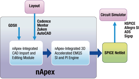
nApex는 업계 표준 형식의 GDS, package 와 board를 불러올 수 있으며, workspace안에서의 통합기능을 제공합니다. 또한 DC와 skin-depth기반으로 고유의 손실 모델링 기술을
사용하면서 저항과 인덕턴스의 고주파 특성을 해석하고, broadband 특성은 output SPICE 모델에서 single frequency-independent circuit을 이용하여 나타냅니다.
또한 다양한 Features들을 선택하여 사용함으로써 임피던스, 저항, 컨덕턴스, 캐퍼시턴스, 인덕턴스와 완전한 SPICE netlist, skin-effect frequency, place on board, 통합 칩의
전자 특성 결과들을 얻을 수 있고, 기존 디자인 흐름(CAD)와 긴밀하게 통합되어 설계 환경에서 frontend와 backend 프로세스화가 가능합니다.
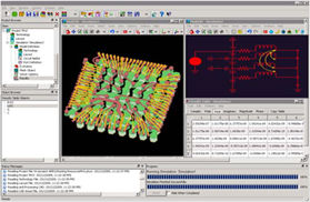
Design Flow
nApex는 보편적인 CAD형식을 직접 불러들임으로써, 같은 framework와 standard CAD flow에 적합한 통합 quasi-static 3D SI와 PI 솔루션을 제공합니다.
Features
■ Accelerated EMQS boundary element technology
■ O(N) memory and time scalability
■ Impedance, resistance, conductance, capacitance, and inductance extraction with skin effect frequency dependence
■ Skin‐effect‐aware broadband SPICE model generation
■ Automatic SPICE model generation
■ Choice of L or π model and number of stages in output netlist
■ Scalable load‐balanced multi‐core compressed accelerated boundary element technology
■ OpenMP‐LSF based integrated hybrid computing platform support
■ Windows and Linux, 32‐bit and 64‐bit
■ Package layout editing and healing
■ Selection by net, region, and cross annotation
■ Cropping by layer and net for 3d tunneling
■ Automated port setup
■ Intuitive pin‐grouping option
■ Stop and resume simulation at any time
■ Chip metal layers, redistribution layer, package and board merging from industrystandard file formats from Cadence, Zuken, AutoCAD, and Mentor
■ Integrated open ASCII database for complete 3d merged model
■ Automatic and intuitive net‐naming propagation and net connectivity check upon merging multiple formats
■ Parametric input through ASCII .bool format
■ Pre‐solve estimate memory function
■ PoP, SiP, MCM, and stacked die support
■ Choice of number of simulation threads and cores for solver, enabling some cores to be left free for other tasks
■ Full 3D control on bond wire, solder ball, solder bump and lead design
■ QFN / QFP package design wizard
■ Cadence Allegro: .mcm, .brd, .sip,
Zuken: .pcb, .rif, Mentor: .hkp,
AutoCAD: .dxf, GDS: .gds, .gdsii, .gds2,
Other: ,cif
■ GDS and CIF import
■ Export models directly to HSPICE, Spectre, SigXP, Allegro SI, Agilent ADS
■ Enhanced 3D drawing frontend for customized and add‐on structures
■ LSF support for task distribution on clusters
■ Extended large number of cores multi‐core and multi‐CPU engine
■ Enhanced passive and causal model tester and SPICE netlist generator
■ Complex BGA and bond‐wire packages
■ Package‐on‐package configurations
■ Systems‐in‐package and MCMs
■ Thru Silicon Via (TSV) modeling
■ Multilayered boards
■ Coplanar packages
■ QFN, QFP, leadframe packages
■ DDR memory interfaces
■ Embedded passives
■ Detailed via, transition, interconnect, bondwire, solder ball, and solder bump modeling
■ Package and board merged
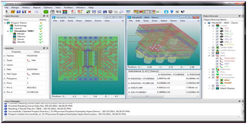
3D EMQS Extraction
Enhanced Usability and GUI Features
Integration with Frontend and Layout Tools
Integration with Circuit Simulators
Extended Options
Applications
샘플 키트는 사용을 위한 준비가 되어 있으며, 고객의 특정 요건들을 충족시키기 위해 쉽게 재설정될 수 있습니다. 이것은 신호 무결성과 타이밍 분석들이 광범위한 기생 변수들의
프로세스, 전압, 온도 조건들에 대해 빠르게 수행될 수 있도록 합니다. 이 외에, on-die termination(ODT)과 slew rate derating이 자동으로 수행되며, 모든 DDR2 파형 프로세싱
레벨들이 지원됩니다.


